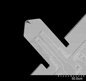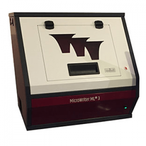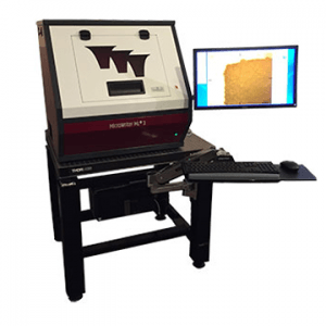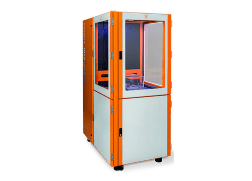
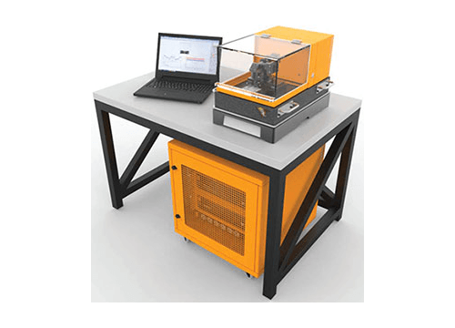
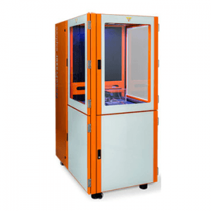
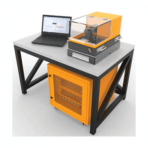
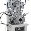

The NanoFrazor is a unique tool for rapid prototyping of 3D nano-structures and nano-devices. The patterning principle of the NanoFrazor technology is based on Thermal Scanning Probe Lithography (t-SPL) which originates from IBM Rueschlikon.
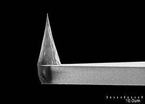
The NanoFrazor uses a hot probe tip to locally heat an organic resist which instantly decomposes into volatile units. The volatile units evaporate and leave arbitrary shaped nanometer sized cavities. The NanoFrazor has been developed for researchers who want to have easy and quick access to high-resolution nanometer sized geometries. Even 3D nano-patterns can be fabricated in a single step with unmatched precision. The closed-loop lithography (CLL) concept of the technology makes the patterning procedure extremely robust at 1 nm vertical resolution. Simultaneous inspection of the written nanostructures allows immediate quality control and feedback. Furthermore the in-situ inspection capability of the NanoFrazor facilitates novel and unique ways for stitching and overlay at sub 5 nm precision.
Features and applications of NanoFrazor Explore and NanoFrazor Scholar
- Direct-write greyscale nanolithography
- In-situ inspection provides additional topography information and accuracy
- No electron damage to sensitive materials
- Precise overlay & stitching capabilities based on imaged topography
- Intuitive and easy to use software interface
- Automatic tip temperature calibration, surface detection and approach
- Low maintenance cost
- Operates in ambient / nitrogen atmosphere